Silicon as a Reference Material for Raman Spectroscopy: Advantages and Challenges
by Dr Enrique Lozano
Overview
Raman spectroscopy is a powerful analytical technique used to study vibrational, rotational, and other low-frequency modes in a material. To ensure accuracy and reliability in Raman spectroscopy measurements, reference materials are crucial. Silicon, a widely used semiconductor, has become a popular choice as a reference material for Raman spectroscopy due to its unique properties. In this application note we will explore the advantages and challenges associated with using silicon in Raman spectroscopy.
Silicon is a crystalline semiconductor characterised by a face-centred cubic structure (FCC). It is widely available and cost-effective, making it accessible for numerous applications.
This material displays a distinct and robust primary Raman band, known as the TO (transverse optical) band, situated around ~520 cm-1 in the low-frequency region. This band originates from the vibration of silicon atoms within the crystal lattice.
Silicon’s transparency to a wide range of wavelengths used in conventional Raman spectroscopy is primarily attributed to its electronic band structure. In a crystalline semiconductor like silicon, the electronic band structure plays a crucial role in determining its optical properties. The concept of a “forbidden energy range” is closely related to the band gap of the material and refers to the energy range between the valence band and the conduction band where electronic transitions are not allowed. When a material has a wide forbidden energy range, it means that the energy required for electronic transitions is high. In silicon, this energy range is significant.
Si as a Reference Material for Raman
In the context of Raman spectroscopy, a wide forbidden energy range is advantageous because it means that silicon is transparent on a broad range of the visible and NIR spectra. In Raman spectroscopy, a laser is typically used to excite the sample, and the scattered light is analysed for information about molecular vibrations. If the material is transparent across a wide range of energies, the incident laser light can effectively penetrate the material without being absorbed.
This transparency allows the laser light to interact with the sample without causing excessive absorption, ensuring that the Raman scattering process is not overshadowed by absorption effects. As a result, silicon’s transparency to the majority of Raman laser wavelengths makes it a preferred material for Raman spectroscopy, enabling efficient and reliable measurements of vibrational modes in a wide range of samples.
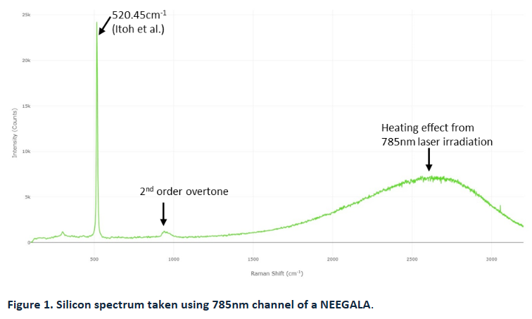
As a reference material in Raman spectroscopy, silicon facilitates laser zeroing calibration, a technique for establishing the Raman shift axis in scenarios where the laser’s precise wavelength is unknown (or can be used to verify precisely). The use of a material exhibiting a consistent and sharp peak enables the back-calculation of the laser wavelength from the wavenumber at which the peak manifests. A study conducted by Itoh et al. estimates that the main silicon band is situated at 520.45 ± 0.28 cm-1 for Si 100.
Some advantages of using crystalline Si as a reference material:
1. Sharp and clear Raman Peaks:
Crystalline Silicon exhibits a well-defined Raman peak (1 peak only – in some devices, overtones are visible and should not be mistaken with the peaks of amorphous Si), making it an excellent reference material for calibration purposes. The sharpness of these peaks allows for precise calibration of the Raman spectrometer, enhancing the accuracy of measurements.
2. Homogeneity:
Silicon is homogeneous at the atomic level, ensuring consistent Raman signals throughout the material and across devices and manufacturers. This homogeneity is essential for reproducibility and reliable comparisons between different measurements and instruments.
3. Stability:
Silicon is chemically stable and does not react with common laboratory environments. This non-reactive nature ensures that the reference material remains unchanged over time, reducing the need for frequent recalibration and product recertifications.
4. Accessibility:
Silicon samples are broadly accessible and economical to purchase. The well-defined crystal structure is easily verified and traceable.
Challenges Regarding the use of Silicon as a Reference Material
Even if Si looks like a perfect and ideal material, it is necessary to mention some challenges:
1. Laser wavelength stability
Silicon’s Raman spectrum is highly sensitive to the laser wavelength used. Small variations in the laser line can cause shifts in the silicon Raman peaks, potentially leading to inaccuracies in calibration. Careful selection and stabilisation of the laser source are necessary to mitigate this challenge. It means that a laser which is not stable will provide different read outs of the Si. This can be used indirectly by users to evaluate the quality of the Raman lasers.
2. Thermal Effects
Silicon undergoes a temperature-dependent shift in its Raman spectrum, known as thermal expansion. This effect can introduce uncertainties in measurements, especially when working with samples at elevated temperatures or when using high level of power in the Raman device. Temperature control and compensation methods are required to address this challenge. Paying close attention to the optical setup used in the measurement is particularly important, as the laser’s power density can affect the local temperature of the sample and cause the signal to drift slightly.
3. Fluorescence Interference:
Silicon can exhibit weak fluorescence, particularly when excited with shorter wavelengths. Fluorescence can overlap with Raman peaks, complicating the analysis. This issue may be mitigated by using longer excitation wavelengths or advanced techniques, such as time-resolved Raman spectroscopy.
4. Surface Roughness:
The surface roughness of silicon samples can impact Raman measurements, leading to the broadening of peaks and potential interference. Ensuring a smooth and uniform silicon surface is crucial to minimize this effect.
Conclusion
Silicon serves as an excellent reference material for Raman spectroscopy, offering sharp and well-defined peaks along with homogeneity. While challenges such as laser line sensitivity and thermal effects exist, careful experimental design and calibration strategies can effectively address these issues. Overall, the advantages of using silicon as a reference material often outweigh the challenges, making it a valuable choice for ensuring the accuracy and reliability of Raman spectroscopy measurements.
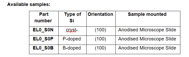
ELODIZ offers a range of Si-certified samples (microscope side mount) that can be used as reference tool in Raman spectroscopy to evaluate laser stability or to validate the excitation wavelength of any Raman device.